MC33178 MC33179
HIGH OUTPUT CURRENT LOW POWER, LOW NOISE OPERATIONAL AMPLIFIERS
The MC33178/9 series is a family of high quality monolithic amplifiers employing Bipolar technology with innovative high performance concepts for quality audio and data signal processing applications. This device family incorporates the use of high frequency PNP input transistors to produce amplifiers exhibiting low input offset voltage, noise and distortion. In addition, the amplifier provides high output current drive capability while consuming only 420 µA of drain current per amplifier. The NPN output stage used, exhibits no deadband crossover distortion, large output voltage swing, excellent phase and gain margins, low open–loop high frequency output impedance, symmetrical source and sink AC frequency performance.
The MC33178/9 family offers both dual and quad amplifier versions, tested over the vehicular temperature range, and are available in DIP and SOIC packages.
• 600 Ω Output Drive Capability
• Large Output Voltage Swing
• Low Offset Voltage: 0.15 mV (Mean)
• Low T.C. of Input Offset Voltage: 2.0 µV/°C
• Low Total Harmonic Distortion: 0.0024% (@ 1.0 kHz w/600 Ω Load)
• High Gain Bandwidth: 5.0 MHz
• High Slew Rate: 2.0 V/µs
• Dual Supply Operation: ±2.0 V to ±18 V
• ESD Clamps on the Inputs Increase Ruggedness without Affecting Device Performance
MAXIMUM RATINGS
| Rating | Symbol | Value | Unit |
| Supply Voltage (VCC to VEE) | VS | +36 | V |
| Input Differential Voltage Range | VIDR | (Note 1) | V |
| Input Voltage Range | VIR | (Note 1) | V |
| Output Short Circuit Duration (Note 2) | tSC | Indefinite | sec |
| Maximum Junction Temperature | TJ | +150 | °C |
| Storage Temperature Range | Tstg | –60 to +150 | °C |
| Maximum Power Dissipation | PD | (Note 2) | mW |
NOTES:
1. Either or both input voltages should not exceed VCC or VEE.
2. Power dissipation must be considered to ensure maximum junction temperature (TJ) is not exceeded. (See power dissipation performance characteristic, Figure 1.)

ORDERING INFORMATION
| Op Amp Function | Fully Compensated | Operating Temperature Range | Package |
| Dual | MC33178D MC33178P | TA = –40°C to +85°C | SO–8 Plastic DIP |
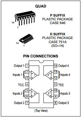
| Quad | MC33179D MC33179P | TA = –40°C to +85°C | SO–14 Plastic DIP |


Product Tags:

|
|
MC33179D amplifier ic chip Integrated Circuit Chip HIGH OUTPUT CURRENT LOW NOISE OPERATIONAL AMPLIFIERS Images
|